Design of Two Stage Operational Amplifier 45nm CMOS Process in Cadence Virtuoso step by step Process

Two Stage OTA CMMR Calculation Using Cadence VirtuosoПодробнее

Two Stage OTA AC Analysis Using Cadence VirtuosoПодробнее

Design of a Differential Amplifier 45nm CMOS Process in Cadence Virtuoso | Part IIПодробнее

Analog VLSI Custom Layout Cadence Virtuoso Differential Pair-Part 3 (Routing and Current matching)Подробнее

Design of a Differential Amplifier 45nm CMOS Process in Cadence Virtuoso | Part OneПодробнее

CMOS Two-Stage Operational Amplifier schematic & symbol in Cadence VirtuosoПодробнее

An Design & Analysis Of Multi Stage Op-Amp Using Cadence - 1Подробнее

Why used Dummy Mosfet in Analog Layout VLSI (Cadence)| What is Well Proximity Effect (WPE) in VLSIПодробнее

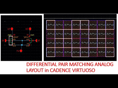
Differential Pair Analog Layout and Matching Techniques in Cadence Virtuoso in 45nm CMOS | Part-1Подробнее