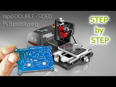
Double layer PCB prototyping 0.1 mm traces/spaces
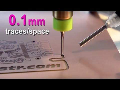
Double layer PCB prototyping 0 1 mm traces spacesПодробнее

PCB Manufacturing and Assembly Process in Factory | How Printed Circuit Boards are Made | ProductionПодробнее
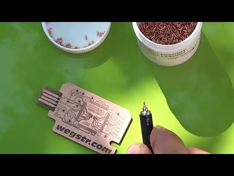
PCB making - double layer PCB prototyping - E-paper displayПодробнее

PCB making, PCB prototyping how to make a PCB 4mil 0 1mm traces space step by step PART 2 1080Подробнее

PCB making and PCB prototyping - 0.05 mm traces/spacesПодробнее

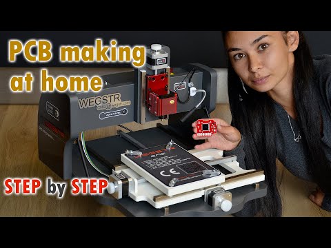
PCB prototyping, PCB making at home - WEGSTRПодробнее
Salsa Night in IIT Bombay #shorts #salsa #dance #iit #iitbombay #motivation #trending #viral #jeeПодробнее

Connectivity of PCB Layers, vias on a home-made PCBПодробнее
PCB prototyping with UV solder-mask. High precision PCB double-sided. Chips QFN36 and ATMEGA 328P-AUПодробнее
1st yr. Vs Final yr. MBBS student 🔥🤯#shorts #neetПодробнее

UPSC VS IIT JEE 🥵 #iitstatus #motivation #toppers #iitjee #jeemains #upscstatus #neet #nit #jeeПодробнее

PCBWay - How to make a 2-layer PCB (full version)Подробнее

The Wegstr CNC prototyping millПодробнее
